Lumen Future provides precision semiconductor laser processing services in Singapore, supporting semiconductor manufacturers, electronics companies, and precision engineering businesses with advanced laser cutting and fabrication solutions.
Semiconductor laser processing is an advanced manufacturing method that uses focused laser energy to cut, modify, and fabricate precision components used in semiconductor and electronics industries. In Singapore, Lumen Future provides semiconductor laser processing solutions including PI film cutting, thin metal processing, stainless steel parts fabrication, precision brackets, and custom fixtures for advanced manufacturing applications.
What Is Semiconductor Laser Processing?
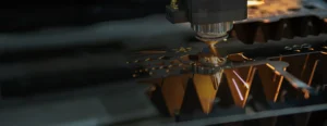
Semiconductor laser processing refers to the use of advanced laser technology to cut, shape, drill, mark, or modify precision materials used in semiconductor manufacturing and electronics production.
Unlike traditional machining methods that rely on physical cutting tools, laser processing is a non-contact manufacturing technology. This allows manufacturers to process thin materials, complex geometries, and delicate components with high accuracy and minimal mechanical stress.
For semiconductor and electronics manufacturers, laser processing is widely used because modern components require:
- High dimensional accuracy
- Fine feature processing
- Consistent production quality
- Minimal material deformation
- Flexible prototype and production capability
Lumen Future provides semiconductor laser processing solutions in Singapore, helping manufacturers produce precision components for semiconductor equipment, electronics applications, and advanced manufacturing systems.
Why Singapore Semiconductor Manufacturers Need Precision Laser Processing
Singapore has one of the world’s strongest semiconductor and electronics manufacturing ecosystems, supported by semiconductor fabrication companies, electronics manufacturers, equipment suppliers, and precision engineering companies.
As semiconductor technology continues to advance, manufacturers require components with tighter tolerances, thinner materials, and more complex designs. Traditional fabrication methods may become challenging when processing:
- Ultra-thin films
- Precision metal components
- Heat-sensitive materials
- Small and complex geometries
- Custom engineering parts
High Precision Requirements
Semiconductor manufacturing equipment requires extremely accurate components to maintain stable production performance.
Laser processing helps manufacturers achieve:
- Accurate dimensions
- Repeatable processing results
- Complex design flexibility
- Reduced tooling limitations
Processing of Advanced Materials
Semiconductor applications often involve advanced materials that require careful processing control, including:
- PI film
- Stainless steel
- Aluminum
- Quartz glass
- Ceramic materials
Selecting the correct laser process is important to control edge quality, thermal effects, and overall component performance.
Support for Prototype to Production Manufacturing
Singapore semiconductor companies frequently require flexible manufacturing support, from engineering prototypes to production quantities.
Laser processing provides advantages for:
- Rapid prototype development
- Small batch manufacturing
- Design modifications
- Production component fabrication
Semiconductor Laser Processing Capabilities
Lumen Future provides semiconductor laser processing services in Singapore for different materials and component requirements.
Semiconductor Laser Processing Services
PI Film Laser Cutting for Semiconductor and Electronics Applications
Polyimide (PI) film, commonly known as Kapton®, is widely used in semiconductor and electronics manufacturing because of its excellent thermal resistance, electrical insulation properties, and chemical stability.
Traditional mechanical cutting methods may create challenges when processing thin flexible materials. Laser cutting provides a precise and flexible solution for producing complex PI film components.
Advantages of PI Film Laser Cutting
- Precise cutting of thin film materials
- Ability to create complex patterns and small features
- Reduced mechanical deformation
- Flexible production for prototypes and customized designs
- Consistent repeatability for manufacturing
PI Film Applications in Semiconductor Manufacturing
- Flexible circuit components
- Insulation layers
- Electronic protection films
- Semiconductor-related precision components
Learn more about PI film processing:
PI Film Laser Cutting Guide for FPC and Electronics Manufacturing
Thin Metal Laser Cutting for Semiconductor Components
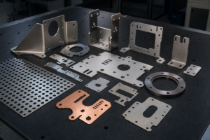
Semiconductor equipment and electronics manufacturing require thin metal components with high precision, excellent edge quality, and consistent production performance.
Lumen Future provides thin metal laser cutting services in Singapore for semiconductor-related components, supporting manufacturers that require reliable fabrication solutions for complex and precision parts.
Common thin metal materials used in semiconductor applications include:
- Stainless steel
- Aluminum
- Copper
- Titanium alloy
Advantages of Thin Metal Laser Cutting
- High dimensional accuracy for precision components
- Ability to process complex geometries
- Reduced mechanical stress compared with traditional cutting
- Suitable for prototype and production manufacturing
- Flexible design changes without expensive tooling
Thin Metal Semiconductor Component Applications
| Component Type | Application |
|---|---|
| Precision Brackets | Mounting and positioning semiconductor equipment components |
| Equipment Covers | Protective structures for semiconductor machinery |
| Metal Shields | Electronic and electromagnetic protection applications |
| Custom Mechanical Parts | OEM semiconductor equipment manufacturing |
Precision Stainless Steel Parts Fabrication for Semiconductor Equipment
Stainless steel is widely used in semiconductor manufacturing equipment because of its excellent corrosion resistance, durability, and stable mechanical properties.
For semiconductor applications, stainless steel components often require precise dimensions, clean edges, and consistent quality to ensure reliable equipment performance.
Stainless Steel Laser Processing Applications
- Semiconductor equipment brackets
- Machine support structures
- Precision panels and covers
- Custom fabricated components
- Assembly fixtures
Stainless Steel Processing for Semiconductor Applications
Custom Brackets and Fixtures for Semiconductor Manufacturing
Semiconductor manufacturing equipment requires many customized mechanical components to maintain accurate positioning, stable operation, and efficient production processes.
Lumen Future supports semiconductor companies with customized laser fabricated brackets and fixtures designed according to engineering drawings and application requirements.
Typical Semiconductor Fixture Applications
- Positioning fixtures
- Assembly support brackets
- Equipment mounting components
- Custom tooling parts
- Machine modification components
- Design Flexibility: Custom components can be produced according to specific equipment requirements.
- Fast Prototyping: Laser fabrication allows faster development of engineering samples.
- Production Support: Suitable for low-volume and repeat manufacturing projects.
- Precision Control: Consistent processing supports demanding semiconductor applications.
Materials Processed for Semiconductor Laser Applications
Semiconductor and electronics manufacturers use a wide range of advanced materials. Each material requires appropriate laser parameters and processing methods to achieve the required quality.
| Material | Laser Processing Applications |
|---|---|
| PI Film | Flexible electronics, insulation layers, FPC-related components |
| Stainless Steel | Semiconductor equipment parts, brackets, fixtures, and covers |
| Aluminum | Lightweight structures and precision mechanical components |
| Copper | Electronic components and conductive parts |
| Quartz Glass | Optical and semiconductor-related applications |
| Sapphire | Precision transparent components and advanced industrial parts |
| Ceramic | High-temperature semiconductor equipment applications |
Different materials require different processing approaches. Lumen Future evaluates material properties, thickness requirements, and application needs to recommend suitable laser processing solutions.
Related processing capabilities:
- Precision Glass Laser Processing in Singapore
- Ceramic Laser Processing Singapore
- Laser Cutting Services Singapore Buyer Guide
Semiconductor Applications Supported by Lumen Future
Lumen Future supports semiconductor and electronics manufacturers in Singapore with customized laser processing solutions for different manufacturing requirements.
Semiconductor Equipment Components
Laser processed components are commonly used in semiconductor equipment manufacturing, including:
- Equipment covers
- Precision brackets
- Support structures
- Custom fixtures
- Mechanical components
Electronics Manufacturing Applications
Laser processing supports electronics manufacturers with precision parts used in:
- Flexible electronics
- Thin film components
- Electronic protection parts
- Customized precision components
Precision Engineering Applications in Singapore
Singapore has a strong precision engineering sector supporting semiconductor, electronics, and advanced manufacturing industries.
Lumen Future works with precision engineering companies requiring:
- Custom fabricated parts
- Prototype development
- Small batch manufacturing
- Production component supply
Learn more about our semiconductor industry capabilities:
Quality Requirements for Semiconductor Laser Processing
Semiconductor manufacturing requires strict control over component quality because even small variations can affect equipment performance, assembly accuracy, and production reliability.
For semiconductor laser processing applications, manufacturers usually focus on three key quality factors:
Dimensional Accuracy and Repeatability
Precision semiconductor components require accurate dimensions and consistent manufacturing results.
Laser processing helps achieve stable production through controlled parameters, allowing manufacturers to produce components with:
- Consistent dimensions
- Repeatable processing quality
- Complex design capability
- Reduced manufacturing variation
Edge Quality and Burr Control
Edge quality is an important consideration for semiconductor components, especially for thin materials and precision mechanical parts.
Laser processing can help reduce:
- Burr formation
- Mechanical deformation
- Additional finishing requirements
Thermal Control During Laser Processing
Sensitive semiconductor materials require careful control of heat input during processing.
Proper laser parameter selection helps minimize:
- Heat affected zones
- Material distortion
- Surface damage
- Material Evaluation: Analyze material properties and application requirements before processing.
- Process Selection: Select suitable laser technology based on thickness, precision, and quality requirements.
- Engineering Review: Verify CAD drawings, dimensions, and manufacturing requirements.
- Quality Inspection: Check finished components for dimensional accuracy and surface quality.
Why Choose Lumen Future for Semiconductor Laser Processing in Singapore?
Choosing the right manufacturing partner is important for semiconductor companies that require precision components, reliable production quality, and responsive engineering support.
Singapore-Based Manufacturing Support
Lumen Future provides laser processing services in Singapore, supporting local semiconductor manufacturers, electronics companies, and precision engineering businesses.
Working with a Singapore-based manufacturing partner provides advantages including:
- Local communication and project coordination
- Faster engineering discussions
- Support for prototype development
- Better understanding of Singapore manufacturing requirements
Advanced Laser Processing Capability
Different semiconductor applications require different laser technologies. Lumen Future provides processing solutions based on material characteristics and application requirements.
Our capabilities include:
- Fiber laser processing for metal components
- UV laser processing for precision applications
- CO₂ laser processing for selected non-metal materials
Prototype to Production Manufacturing Support
Semiconductor companies often require flexible manufacturing support throughout different development stages.
Lumen Future supports customers from:
From CAD File to Finished Component
How Semiconductor Companies Work With Lumen Future
Step 1: Submit Your Design Requirements
Customers can provide:
- CAD drawings
- DXF files
- 3D models
- Material specifications
- Production requirements
Step 2: Engineering Review
Our team reviews the project requirements, including:
- Material suitability
- Laser processing method
- Manufacturing feasibility
- Quality requirements
Step 3: Precision Manufacturing
After confirmation, components are processed according to customer drawings and application requirements.
Step 4: Quality Verification
Finished components are evaluated based on project requirements, including:
- Dimensional accuracy
- Surface quality
- Processing consistency
Frequently Asked Questions About Semiconductor Laser Processing
Semiconductor laser processing is an advanced manufacturing method that uses focused laser energy to cut, modify, or fabricate precision components used in semiconductor and electronics applications. It enables high accuracy processing of thin materials, complex geometries, and customized parts.
Common materials include PI film, stainless steel, aluminum, copper, quartz glass, sapphire, and ceramic materials. The suitable laser process depends on material properties, thickness, and application requirements.
Laser cutting provides high precision, flexible manufacturing capability, and minimal mechanical stress, making it suitable for semiconductor components, precision fixtures, and thin material processing.
Yes. Lumen Future supports prototype development, engineering samples, low-volume production, and customized semiconductor-related component manufacturing in Singapore.
Yes. Lumen Future provides semiconductor laser processing solutions in Singapore for semiconductor manufacturers, electronics companies, and precision engineering businesses.
Lumen Future supports semiconductor, electronics, industrial automation, precision engineering, and advanced manufacturing industries with customized laser processing solutions.
Need Semiconductor Laser Processing Support in Singapore?
Send your drawings and material requirements to Lumen Future. Our engineering team can review your project requirements and recommend suitable laser processing solutions.
- PI film laser cutting
- Thin metal precision cutting
- Semiconductor parts fabrication
- Custom brackets and fixtures
- Prototype to production support
Lumen Future provides semiconductor laser processing solutions in Singapore, helping manufacturers produce precision components with advanced laser cutting and fabrication technologies.
Whether you require PI film cutting, thin metal processing, stainless steel parts, or customized semiconductor fixtures, our team supports your manufacturing requirements from prototype development to production manufacturing.