Laser PI Film Cutting

Precision PI Film Cutting in Singapore

Burr-free laser cutting for polyimide film, Kapton, flexible PCB substrates, and multi-layer flex circuits. No mechanical stress, no delamination — tolerances from ±0.03 mm for the tightest flex electronics applications, all from our Singapore facility.

Tolerance
± 0 mm
Film Thickness
0 mm
Typical Turnaround
0 h
Film Types
0 +

PI Film & FPC Cutting Samples

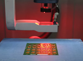
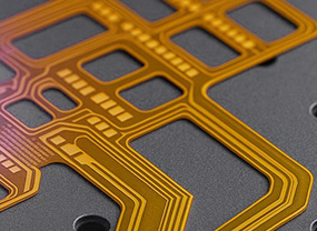
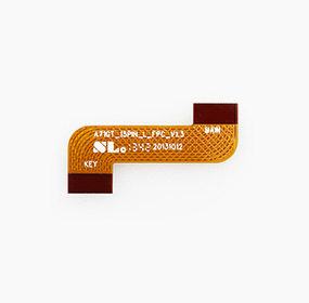
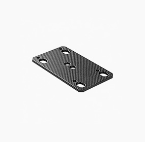
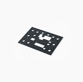
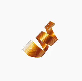
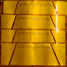
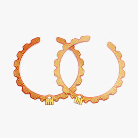
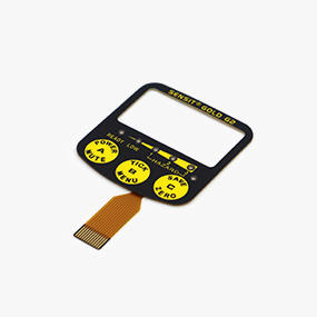
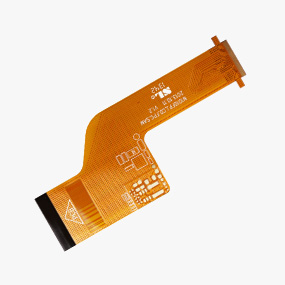
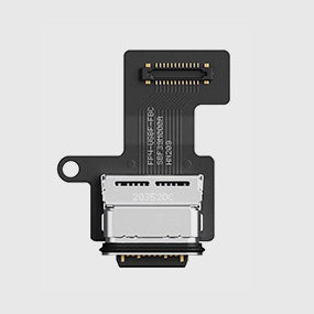
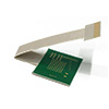
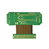
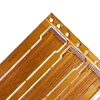
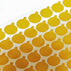
Explore PI film and FPC cutting samples for flexible circuits, insulation films, adhesive-backed polyimide sheets, electronic components, and custom thin-film parts. Our laser PI film cutting service supports fine contours, small holes, clean edges, and prototype-to-small-batch production for electronics and precision manufacturing projects in Singapore.

What We Do

Cutting Capabilities

Our UV and CO₂ laser systems are tuned for thin polymer films — delivering clean, burr-free cuts without the heat distortion, delamination, or micro-tears of mechanical die-cutting.

±0.05mm

Cutting Tolerance

standard; ±0.03mm for fine-pitch FPC on request

Tight positional accuracy maintained across roll-to-sheet and sheet formats. Critical for multi-layer flex alignment.

600×600 mm

Max Sheet / Panel Size

per pass; roll-fed available on request
 

Full-panel processing in one pass. Eliminates repositioning errors on large flex circuit panels.

0.01 – 0.5mm

Film Thickness Range

single layer to multi-layer flex stack

From ultra-thin 10 μm single-layer PI to 0.5 mm multi-layer flex stacks with adhesive and coverlay.

Burr-free

Edge Quality

clean polymer edge, no charring or melt-back

No burrs, no micro-tears, no carbonisation on cut edges. UV laser minimises HAZ on copper traces near cut lines.

UV 355nm

Laser Type

+ CO₂ 10.6 μm — dual capability

UV laser (355 nm) for fine-pitch FPC with copper traces; CO₂ for pure PI film and simple outlines. Both in-house.

0.1mm

Fine Feature Size

minimum slot / feature width

Slots, via outlines, tab cuts, and registration holes as small as 0.1 mm wide. Ideal for FPC routing and coverlay trimming.

Materials

Film Types We Cut

8+ flexible and rigid-flex substrate types processed in-house. Each material has different laser absorption characteristics — our parameters are tuned per film type to prevent delamination, charring, and trace damage.

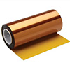
Kapton polyimide film material for precision laser cutting of insulation layers, gaskets and circuit substrates
Most Popular

PI Film (Kapton)

0.013 – 0.25mm

DuPont Kapton HN / EN

Pure polyimide for gaskets, insulation layers, flex heaters and circuit substrates.

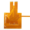
Flexible PCB material with PI, copper and adhesive layers for precision laser cutting
High Demand

Flexible PCB (FPC)

0.05 – 0.3mm

PI + copper + adhesive stack

UV laser preserves copper traces. Single, double-sided and multi-layer.

PI coverlay material with adhesive for precision cutting of FPC protection layers and pad openings
FPC

Coverlay (PI + Adhesive)

0.025 – 0.1mm

Acrylic or epoxy adhesive bonded PI

Precision window and pad opening cuts for FPC protection layers.

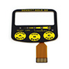
PET film material for laser cutting of membrane switches, label substrates and flexible circuit parts
Membrane

PET Film

0.025 – 0.25mm

Polyester film for membrane switches

label substrates, and low-cost flex circuits. CO₂ laser cutting.

LCP film material for precision laser cutting of 5G, RF and high-frequency flexible substrates
5G / RF

LCP (Liquid Crystal Polymer)

0.05 – 0.2mm

Low dielectric loss, precise cutting needed

High-frequency flex substrate for 5G antennas and mmWave applications.

PI film bonded with stainless steel stiffener for rigid-flex circuit and connector support areas
Rigid-Flex

PI + Stainless Steel (Rigid-Flex)

0.1 – 0.5mm

Stainless steel stiffener bonded to PI

Structural support for connector areas. UV laser cuts both layers clean.

Copper-clad PI film material for flexible circuit substrates and precision outline cutting
Substrate

FCCL (Copper-Clad PI)

0.05 – 0.15mm

Flexible copper-clad laminate before circuit patterning

Blanking and outline cuts for downstream processing.

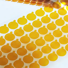
Adhesive-backed PI film tape for laser cutting of gaskets, masks and protective film components
Adhesive

PI Tape / Adhesive Film

0.01 – 0.08mm

Single or double-sided adhesive PI tape

Die-free custom shapes: gaskets, masks, protective film cuts.

Working with a multi-layer stack or unusual substrate? Send us your stackup — we’ll advise on the right laser and confirm capability before you commit.

Where PI Film Cutting is Used

PI film cutting is a core enabling process for flexible electronics — from wearable devices to satellite antennas and medical implants.

Semiconductor & Wafer Handling

Wafer Tape & Process Film Cutting

Dicing tape rings Backgrinding film UV-release tape

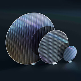
Dicing tape rings, backgrinding film, and UV-release tape cut to wafer carrier dimensions. Precise outline and slot cuts with no adhesive bleed onto cut edges.

Consumer & Wearable Electronics

Flexible Circuit & Antenna Cutting

FPC outlines NFC antenna blanks Wearable flex

FPC outlines, NFC / RFID antenna blanks, wearable flex circuits. UV laser preserves copper traces right up to the cut edge — critical where trace clearance is under 0.2 mm.

Medical Devices

Implantable & Diagnostic Flex Circuits

Catheter flex Neural probes Diagnostic patches

Thin PI flex circuits for catheter tips, neural probes, and diagnostic patches. Biocompatible materials, clean edges, and lot traceability available for regulated production.

Aerospace & Defence

High-Reliability Flex Assemblies

Avionics flex Satellite antennas LCP substrates

LCP and high-Tg PI substrates for avionics flex circuits and satellite communication antennas. Tight tolerances, full dimensional inspection reports on request.

Industrial & Thermal Management

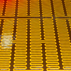
Flex Heaters & Insulation Gaskets

Flex heaters Insulation gaskets Thermal interface

Kapton flex heaters, thermal interface gaskets, and electrical insulation layer cuts. Custom shapes from DXF — no tooling or die setup required even for one-off jobs.

Display & Camera Modules

Display FPC & Camera Flex Cables

ZIF flex tails Camera flex Touch connector

ZIF connector flex tails, camera module flex cables, and touchscreen connector strips. Tight pitch, consistent length, and burr-free edges for automated assembly insertion.

From Drawing to Delivery

Six steps, transparent at every stage. Most orders quote within 24 hours.

What Makes Our PI Film Cutting Different

Thin film cutting is unforgiving — the wrong laser or fixture causes delamination, trace damage, and dimensional shift. We’ve built the process specifically for flex substrates.

Laser Cutting vs Other PI Film Cutting Methods

Understand where laser cutting beats die-cutting and mechanical methods for flexible substrates.

Criterion Laser Cutting (Ours) Steel Rule Die CNC Router Mechanical Punch
Dimensional tolerance ±0.03mm ±0.1–0.3mm ±0.1mm ±0.05mm (with die)
Tooling / NRE cost
None
S$300–2000 per die
None
High (punch + die)
Min order quantity 1 piece 500–5000 pcs MOQ 1 piece 1000+ pcs typical
Copper trace damage
None (UV laser)
Edge crush possible
Heat / burr on traces
Shear stress on traces
Design change lead time
Same day (DXF update)
1–3 weeks (new die)
Same day
1–3 weeks (new punch)
Complex internal features
Yes — any shape
Limited by die design
Yes but slow
Simple shapes only

Featured Projects

PI Film Cutting Work We've Delivered

A selection of recent PI film and flex substrate cutting projects across semiconductor, medical, and consumer electronics.

Services That Work Well Together

PI film cutting is often one step in a broader flex assembly process. We handle what comes next.

FAQ

PI Film Cutting Questions

These are some of the common questions customers ask before sending drawings or requesting quotation.

CO₂ laser (10.6 μm) works well for pure PI film and simple outlines where copper traces are not close to the cut line. UV laser (355 nm) is preferred for FPC with copper layers — its shorter wavelength ablates the polymer without thermally loading the copper, preventing trace discolouration, delamination, and adhesive bleed. For multi-layer flex with tight trace-to-edge clearances under 0.3 mm, UV is the correct choice.

Yes. We regularly cut multi-layer flex stacks in a single pass. Before production we run test cuts on a sample of your stackup to confirm the parameters produce clean inter-layer separation with no adhesive bleed at the cut edge. Please provide your full stackup spec (layer order, thicknesses, adhesive type) when requesting a quote.

Our UV laser can cut slots and features as small as 0.1 mm wide. For internal holes, the minimum diameter is approximately 0.2 mm. Practical minimum varies with film thickness — thicker multi-layer stacks require slightly larger minimum features due to kerf width and material relief. Include your tightest feature dimensions in your drawing and we’ll confirm feasibility at quoting stage.

Yes. For semiconductor and medical customers we provide serialised job records, first-article inspection (FAI) reports with dimensional measurements, and lot traceability documentation. If your application requires specific quality records for PPAP, IPC, or ISO 13485 submissions, please specify this when enquiring so we can confirm what documentation we can provide.

Roll-to-sheet cutting is available on request for standard PI and PET film rolls up to 300 mm wide. We unwind, flatten, and cut to your specified sheet dimensions before laser processing. For high-volume orders requiring continuous roll-fed laser cutting, please contact us to discuss production volume and setup requirements.

DXF is strongly preferred — it preserves your geometry at 1:1 scale with no PDF interpretation issues. For FPC outlines, please supply the board outline layer only (not copper, silkscreen or drill layers). Gerber RS-274X is also accepted for FPC board outlines. Ensure all lines are closed polylines with no gaps or overlapping segments, as open paths cause incomplete cuts.

Blog

PI Film Cutting Work We've Delivered

Get Started

Get a Free Quote Today

Send your drawing or project requirement for review. We can discuss materials, related processing needs and a practical next step for your project.


Confidentiality Note

We understand the value of your design files. The information you submit will be used only for project evaluation, quotation and production communication. We take customer confidentiality, data security and intellectual property protection seriously.