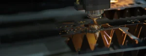
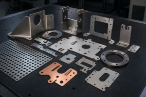
There is no single cutting method that is automatically best for every PI film part. UV nanosecond laser cutting is a strong starting point for fine FPC outlines, coverlay openings and copper-bearing stacks because its short wavelength can reduce thermal loading and support small features. Ultrafast lasers may be considered when the smallest possible heat-affected zone is critical. CO₂ laser cutting can remain practical for selected pure PI films and simpler outlines, while die cutting can be economical for stable, high-volume designs. The correct route must be validated on the actual film, adhesive and layer stack.
PI film—polyimide film, often referred to by the Kapton® trade name—is used in flexible printed circuits, electrical insulation, coverlays, stiffeners, heaters and precision electronics. It is thin, flexible and thermally durable in service, but those same parts can be difficult to cut consistently when adhesives, copper, coatings or multiple layers are involved.
This guide explains how to compare PI film laser cutting with die cutting and other methods, how to recognise carbonisation, adhesive reflow, delamination and dimensional drift, and what FPC engineers and procurement teams should include in a production-ready RFQ. For current equipment capability or a project review, see our PI film cutting service in Singapore.
What Is PI Film—and What Are You Actually Cutting?
Polyimide film combines electrical insulation, dimensional stability, chemical resistance and flexibility. These properties make it useful in electronics, semiconductor equipment, sensors, flexible heaters, medical devices and other assemblies that must operate in demanding thermal or electrical environments. Published Kapton® film information illustrates why PI films are widely specified, but the finished part may behave very differently from a sheet of bare film once adhesives, copper and coatings are added.
In practice, a “PI film cutting” request may refer to any of the following:
| Material or stack | Typical function | What changes the cutting decision |
|---|---|---|
| Bare PI film | Insulation, spacers, masks and flexible components | Film grade, thickness, flatness and acceptable edge colour |
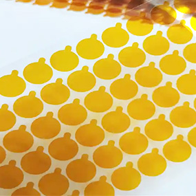
| Adhesive-backed PI | Die-cut-style gaskets, labels, masks and bonding layers | Adhesive chemistry, liner, residue and reflow risk |
| Coverlay | Protects FPC copper traces while exposing selected pads | Window size, registration, adhesive bleed and copper clearance |
| FCCL / copper-clad PI | Flexible circuit substrate | Copper thickness, trace-to-edge distance and selective-depth requirement |
| PI stiffener | Supports connector or component zones | Total thickness, bonded layers and positional tolerance |
| Multi-layer FPC stack | Finished or semi-finished flexible circuit | Layer order, embedded copper, adhesive and acceptance criteria |
PI Film Cutting Methods: Where Each One Fits
A useful comparison does not rank every process from “bad” to “best.” It identifies the production conditions under which each method becomes practical.
| Method | Where it may fit | Main limitations | What to verify |
|---|---|---|---|
| Die cutting / punching | Stable design, simple outlines and high production volume | Tooling cost, design-change delay and possible mechanical stress | Tool tolerance, edge compression, registration and expected tool life |
| Precision knife or mechanical cutting | Simple prototypes and larger features where suitable fixturing is available | Film movement, tearing, tool wear and limited internal geometry | Holding method, minimum radius and batch repeatability |
| CO₂ laser | Selected pure PI films, simple outlines and non-critical edge requirements | Higher thermal load and greater risk of visible charring or adhesive effects | Actual cut sample, edge microscopy and electrical requirement |
| UV nanosecond laser | FPC outlines, coverlay windows, fine features and many adhesive/copper stacks | Not heat-free; results remain sensitive to fluence, overlap and material stack | HAZ, residue, copper condition, registration and cycle time |
| Picosecond / femtosecond laser | Micro-features and applications prioritising very low thermal influence | Higher process cost and less universal equipment availability | Feature requirement, throughput, inspection plan and economic fit |
| Fiber laser | Generally not the first-choice process for PI film | Thermal damage and material-response risks | Use only when testing on the production stack proves the required result |
Laser cutting is attractive for prototypes and frequently revised designs because it does not require a dedicated hard tool. Die cutting can become more economical once geometry and demand are stable enough for tooling cost to be spread across a large volume. Many product programmes therefore use laser cutting during development and qualification, then compare laser and die economics again at production scale.
CO₂, UV and Ultrafast Lasers: What Actually Changes?
Laser wavelength and pulse duration influence how energy is absorbed and how much time heat has to spread into the surrounding film. They are important variables, but they are not the only variables. Fluence, pulse overlap, repetition rate, focus position, scan strategy, exhaust, fixture design and the material stack all affect the finished edge.
CO₂ laser: useful in a narrower PI window
A CO₂ laser operates at a much longer wavelength than a UV laser and removes polymer primarily through a thermal process. It can cut selected bare PI films and simple shapes, but engineers should expect a larger thermal process window and should not assume that results from bare film will transfer to an adhesive-backed or copper-bearing FPC stack.
CO₂ may still be commercially sensible when the geometry is simple, the edge is not adjacent to an electrical feature and a tested sample meets the drawing. It should not be rejected—or approved—solely from the laser name.
UV nanosecond laser: the common precision starting point
A 355 nm UV laser offers shorter-wavelength energy that can be focused into small features and can reduce lateral thermal influence compared with longer-wavelength thermal cutting. This makes it a strong candidate for FPC profiling, coverlay windows, PI stiffeners, adhesive-backed films and features close to copper.
Picosecond and femtosecond lasers: when micro-features justify them
Shorter pulses deposit energy over less time, which can reduce heat diffusion and improve edge control in demanding micro-processing. That capability is valuable for very small holes, narrow slots or high-reliability parts where a nanosecond process cannot meet the acceptance criteria. It is not automatically the lowest-cost choice for every outline, so the extra capability should be tied to a measurable requirement.
How to choose without relying on generic capability numbers
Generic statements such as “less than 5 µm HAZ,” “carbonisation-free” or a fixed positional tolerance are incomplete unless they identify the material, thickness, stack, equipment, measurement method and test conditions. Ask the supplier to confirm the capability against your drawing and production material.
Four Common PI Film Cutting Defects—and How to Control Them
The four failure modes below are more useful than a simple “UV versus CO₂” label because they tell engineering and quality teams what to inspect.
1. Adhesive reflow or edge residue
Adhesive-backed PI can leave a bead, smear or sticky residue along the cut perimeter when the adhesive softens or decomposes. The result depends on adhesive chemistry, liner, cut sequence and thermal input—not only on the PI layer.
Production stack sample
Inspect the edge with the actual adhesive and liner. Confirm cleanliness after handling, not only immediately after cutting.
Bare-film assumptions
A clean result on bare PI does not prove that an acrylic- or epoxy-backed film will behave the same way.
2. Edge delamination
PI, adhesive and copper expand and absorb energy differently. A cut can look acceptable from above while a layer interface has started to separate. For critical stacks, evaluate the edge under magnification and consider whether the finished assembly will experience lamination, solder reflow, bending or thermal cycling.
3. Carbonisation and discolouration
Excessive energy or unsuitable parameters can leave a darkened edge or carbon-rich residue. Where PI is an electrical insulator, this is more than a cosmetic concern: severe carbonisation may reduce insulation performance or create an unacceptable contamination risk. Define whether acceptance is visual, dimensional, electrical—or a combination of all three.
4. Corner overburn and dimensional drift
The beam changes speed around small radii, corners and dense features. If power and motion are not compensated, these zones may receive more energy than a long straight cut. This can enlarge internal corners, shift feature position or create inconsistent kerf width. First-article dimensional data should include the tightest corners and smallest features, not only the overall length and width.
| Defect | Useful inspection | Typical process response |
|---|---|---|
| Adhesive reflow | Edge microscopy, cleanliness and liner-removal check | Adjust energy, overlap, cut order, fixturing or process type |
| Delamination | Magnified edge or cross-section; functional flex test where required | Reduce thermal loading and validate the bonded stack |
| Carbonisation | Visual standard, microscope and electrical test when relevant | Optimise fluence, speed, focus, pulse strategy and extraction |
| Dimensional drift | First-article measurement of corners, holes and critical datums | Apply path, corner and kerf compensation |
Which Process Fits Which PI or FPC Application?
| Application | Common starting point | Critical question |
|---|---|---|
| Bare PI insulation shape | CO₂ or UV trial; die cutting for stable high volume | What edge colour, residue and tolerance are acceptable? |
| Adhesive-backed gasket or mask | UV trial or die cutting depending volume | Does the adhesive reflow or contaminate the edge? |
| FPC outline / depaneling | UV nanosecond; ultrafast if the requirement justifies it | How close are copper traces to the cut line? |
| Coverlay opening | UV process with controlled registration and depth | Must the process stop before copper or expose a pad? |
| Micro-hole or narrow slot | UV or ultrafast laser after feasibility test | What is the measurable minimum feature and allowable taper? |
| High-volume stable outline | Compare validated laser cost with die-cut tooling economics | How often will the design change and what is the annual volume? |
For projects involving FPCs, wafer-handling insulation, sensors or electronics manufacturing, see our semiconductor and electronics application capabilities. If the decision includes metal, glass or other polymers as well as PI, our fiber, CO₂ and UV process-selection guide explains the broader material-to-laser relationship.
How to Validate a PI Film Cutting Supplier
A supplier should be evaluated on evidence from a relevant material stack, not a generic sample or an unsupported machine specification.
- Identify the proposed process. Ask for wavelength and pulse class, but treat them as the start of the discussion—not proof of quality.
- Test the actual stack. Provide the production PI, adhesive, copper and liner whenever possible.
- Define edge acceptance. State whether charring, discolouration, residue or adhesive bleed is permitted.
- Request first-article measurements. Include the smallest hole, tightest corner, critical datum and trace-to-edge distance.
- Confirm inspection method. Dimensional inspection, microscopy and electrical checks answer different questions.
- Clarify documentation. Specify material certificates, FAI, lot traceability, inspection reports and packaging requirements before quotation.
- Review production economics. Compare setup, tooling, inspection and unit cost at the real batch quantity.
For an overview of inspection records and dimensional verification, review our quality assurance process.
PI Film Prototyping and Production in Singapore
Singapore’s semiconductor and advanced-manufacturing ecosystem creates regular demand for flexible circuits, insulation films, process components and precision prototypes. The Singapore Economic Development Board identifies semiconductors as a strategic industry spanning manufacturing, equipment, packaging and related engineering capabilities.
Local PI film processing is valuable when it shortens the engineering feedback loop. The practical benefits are not created by adding “Singapore” to a title; they come from faster material handover, easier review of the actual stack, direct discussion of failure criteria and fewer cross-border shipping or customs variables during prototype iteration.
Where Local Processing Adds the Most Value
Fast design feedback
Review critical geometry, deliver the actual film stack and revise the DXF or Gerber outline after first-article inspection.
Sample-based approval
Agree on edge microscopy, dimensions, trace clearance and documentation before releasing the full batch.
Clear logistics planning
Coordinate local delivery or collection against material availability, inspection scope and the confirmed production schedule.
Do not treat a fixed “48-hour prototype” statement as universal. Turnaround depends on material availability, drawing completeness, the need for test cuts, inspection requirements and batch size. Check current commitments on our Singapore logistics and lead-time page or confirm them during quotation.
What to Include in a PI Film Cutting RFQ
A complete RFQ reduces technical assumptions and makes quotations easier to compare.
Material: Manufacturer, grade and colour
Layer stack: PI / adhesive / copper / coating / liner
Thickness: Each layer and total stack thickness
Drawing: DXF or Gerber outline at 1:1 scale
Critical geometry: Minimum hole, slot, radius and trace-to-edge clearance
Tolerance: Identify critical dimensions rather than applying one tight tolerance everywhere
Quantity: Prototype quantity, batch quantity and expected annual demand
Acceptance: HAZ, edge colour, carbonisation, residue, delamination and burr requirements
Inspection: FAI, microscopy, dimensional report or electrical check
Documentation: Material certificate, lot traceability and packaging requirement
Delivery: Required date and Singapore delivery or self-collection preference
Before sending the file, make sure the intended cut path is unambiguous. Our CAD file preparation guide explains how to remove duplicate lines, close profiles and identify critical dimensions.
Frequently Asked Questions
Is UV laser the only way to cut PI film?
No. UV laser is a strong choice for precision FPC, coverlay and copper-bearing stacks, but selected bare PI films may be cut with CO₂, simple parts may be mechanically cut, and stable high-volume outlines may suit die cutting. The correct method depends on the material stack, geometry, acceptance criteria and volume.
Does UV “cold processing” produce zero heat-affected zone?
No process should be assumed to create zero thermal influence without measurement. UV can reduce heat diffusion compared with longer-wavelength thermal cutting, but HAZ and residue still depend on pulse duration, fluence, overlap, focus, film thickness and the complete layer stack.
Can PI film be laser cut without damaging nearby copper?
It may be possible with the correct wavelength, parameter window, registration and depth strategy, but the result must be validated against the actual FPC stack and trace-to-edge distance. State clearly whether the job is through-cutting, coverlay opening or selective layer removal.
What causes black or carbonised PI film edges?
Excessive or poorly controlled energy input can thermally decompose the polymer and leave dark residue. Laser type matters, but scan speed, pulse overlap, focus, extraction, thickness and adhesive also affect the result. Define the visual or electrical acceptance standard before production.
What file format should I send for FPC or PI film cutting?
DXF is commonly used for a 2D cut outline, while Gerber may be suitable for FPC-related geometry. Supply a clearly identified board-outline or cut-path layer at 1:1 scale, plus a dimensioned PDF showing critical tolerances and datums.
How quickly can a PI film prototype be produced in Singapore?
Lead time depends on material availability, drawing quality, whether a process trial is required, the inspection plan and quantity. Confirm the schedule after the supplier has reviewed the production stack and acceptance criteria rather than relying on a generic turnaround promise.
Should I use laser cutting or die cutting for production volume?
Laser cutting avoids dedicated tooling and supports rapid design changes. Die cutting can reduce unit cost for a stable, simple design at sufficiently high volume. Compare tooling, revision risk, inspection, scrap and annual quantity—not unit price alone.
Validate Your PI or FPC Stack Before Production
Send the actual layer stack, drawing, quantity and acceptance criteria. We can review the geometry, recommend a practical trial route and confirm what inspection evidence is appropriate.
- PI, Kapton®, coverlay, FCCL and adhesive-backed film review
- Prototype and small-batch process assessment
- Dimensional, edge-quality and documentation requirements