Precision glass cutting for industrial use in Singapore — semiconductor windows, optical components, medical device glass, LED substrates — has almost nothing in common with construction glass cutting. It requires UV or ultrafast lasers (picosecond, femtosecond) rather than mechanical scoring, achieves edge chip below 50 µm, and handles specialty materials like borosilicate, quartz, sapphire, and microcrystalline glass (MCG). This guide covers the five industrial glass families you’ll encounter, the four laser technologies used to cut them, achievable tolerances, and where this work matters in Singapore’s semiconductor and photonics clusters.
When a semiconductor process engineer in Singapore needs a 1mm borosilicate viewport with a 50 µm chip-free edge, or an optics designer needs sapphire windows for a high-power laser, the local supplier list shrinks fast. Most “glass cutting” services in Singapore serve HDB windows, kitchen backsplashes, and shopfront fit-outs — not the precision specs that industrial work demands.
This guide is for the other audience: engineers and procurement teams sourcing precision glass parts for semiconductor equipment, photonics modules, medical devices, LED substrates, and lab instrumentation. It covers the five industrial glass materials you’ll most often work with, the four laser technologies used to cut them, what tolerances and edge quality are realistic, and how to specify a quote that gets a useful answer back.

If you’re new to laser-based fabrication in Singapore, our complete laser cutting buyer’s guide covers the basics across all materials, and our supplier selection guide covers how to evaluate fabrication partners more broadly. This piece zooms into glass.
Why Precision Glass Cutting Is Different from Construction Glass
The two are different industries with different equipment, tolerances, and price ranges. A clear comparison:
| Dimension | Construction Glass Cutting | Precision Industrial Glass Cutting |
|---|---|---|
| Typical tolerance | ±1 mm | ±0.05 mm or tighter |
| Thickness range | 3–12 mm | 30 µm to 5 mm |
| Edge quality | Chamfered, polished by hand | Micron-level chip control (<50 µm) |
| Method | Scoring + thermal/mechanical break, water-cooled saw | UV / picosecond / femtosecond laser, controlled fracture |
| Material range | Soda-lime, tempered float glass | Borosilicate, quartz, sapphire, MCG, chemically tempered |
| Pricing structure | Per square metre | Per piece, often 100× higher |
If your application is anything that touches an electron, a photon, a chemical process, or biological tissue — you’re in the precision column. Everything below in this guide assumes that.
5 Industrial Glass Materials in Singapore Projects
The five glass families below cover the vast majority of precision work we see in the Singapore market. Each has distinct properties and matching applications.
Borosilicate Glass (Borofloat 33, Pyrex)
Borosilicate is the workhorse of industrial glass — low thermal expansion, excellent chemical resistance, optically clear. It’s what laboratory glassware, semiconductor reaction chambers, and most viewport windows are made of.
Common in semiconductor process equipment, lab instruments, optical windows
Quartz / Fused Silica
Pure silicon dioxide. Near-zero thermal expansion, extremely high working temperature, and exceptional UV transmission down to 180 nm. Quartz is used wherever deep UV light or high temperatures are involved — semiconductor lithography, photolithography masks, high-temperature furnace ware.
Common in deep-UV optics, semiconductor wafer carriers, high-temperature applications
Sapphire (Single-Crystal Al₂O₃)
Sapphire isn’t glass in the chemical sense — it’s crystalline aluminium oxide with a Mohs hardness of 9, second only to diamond. That hardness is exactly why it’s used where regular glass fails: LED substrates that run hot, scratch-resistant watch crystals, semiconductor process windows exposed to plasma and aggressive chemistry, and laser optics that handle high power density.
Common in LED substrates, semiconductor windows, scratch-resistant optics
Microcrystalline Glass (MCG / Glass-Ceramic)
A composite material — partially crystallised glass with engineered crystal structure. The result is exceptional mechanical strength, near-zero thermal expansion (in some grades), and dimensional stability across temperature swings. Used in aerospace optics, semiconductor wafer carriers, and precision metrology platforms.
Common in aerospace optics, semiconductor carrier wafers, metrology platforms
Chemically Tempered Glass (Gorilla-Class)
Soda-lime or aluminosilicate glass strengthened by ion exchange — sodium ions replaced by potassium ions, creating a compressive surface layer. Common in smart device screens, AR/VR optics, and any consumer-grade application requiring impact resistance.
Common in smartphone displays, smart watches, AR/VR optics, cover glass
For a wider look at materials we work with across all categories, see our materials reference page.
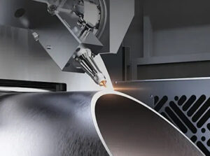
4 Laser Technologies for Cutting Glass: How to Choose
Glass cutting isn’t one laser process — it’s four different technologies, each suited to different material types and quality requirements. Understanding the trade-offs lets you specify the right approach for your project.
CO₂ Laser (10.6 µm wavelength)
Long-wavelength infrared. Glass strongly absorbs CO₂ wavelengths, allowing controlled fracture cutting through thermal stress. Cost-effective for thicker borosilicate, but produces a measurable heat-affected zone (HAZ) and is unsuitable for tempered glass or sapphire.
- Best for: Borosilicate 1–5mm, thick optical glass, lab glassware
- Limitations: HAZ ~100 µm, not suitable for tempered or thin glass
- Edge quality: Smooth on borosilicate, may need polishing for optical applications
UV Nanosecond Laser (355 nm wavelength)
Short wavelength enables direct ablation with minimal thermal impact — often called “cold cutting” even though it isn’t truly athermal. The workhorse for most industrial glass cutting because it balances cost, speed, and quality.
- Best for: Borosilicate, quartz, MCG, thin glass 0.3–3mm
- Limitations: Still produces some chip on hard materials like sapphire
- Edge quality: Chip size 10–50 µm typical
Picosecond Laser (10⁻¹² s pulse duration)
Ultrashort pulses deposit energy faster than heat can diffuse, creating a “cold ablation” effect. Essential for sapphire, chemically tempered glass, and any material where thermal damage must be eliminated.
- Best for: Sapphire, tempered glass, ultra-thin glass (<0.5mm)
- Limitations: Slower than UV ns, higher cost per part
- Edge quality: Chip size <10 µm typical
Femtosecond Laser (10⁻¹⁵ s pulse duration)
The current state of the art. Pulse duration shorter than the electron-phonon coupling time means essentially no thermal damage at all. Used for the most demanding applications — wafer dicing, smartphone cover glass, micro-optics.
- Best for: Sub-millimetre features, wafer-level dicing, ultrathin glass, cover glass for displays
- Limitations: Highest cost per part, slower than picosecond for thick material
- Edge quality: Sub-µm precision, chip size often <5 µm
Matching glass type to laser technology
Tolerances, Edge Quality & What’s Actually Achievable
Industry-typical performance by laser technology. Use these as reference benchmarks when specifying your project:
| Laser Technology | Kerf Width | Dimensional Tolerance | Edge Chip Size | Thickness Range |
|---|---|---|---|---|
| CO₂ Laser | ~100 µm | ±0.05 mm | 50–200 µm | 0.5–10 mm |
| UV Nanosecond | ~30 µm | ±0.025 mm | 10–50 µm | 0.3–3 mm |
| Picosecond | ~20 µm | ±0.015 mm | <10 µm | 0.05–2 mm |
| Femtosecond | ~10 µm | ±0.005 mm | <5 µm | 0.03–1 mm |
Four edge quality terms to know when specifying:
- Chip size — Maximum dimension of edge fragmentation, measured under microscope. Critical for optical performance and downstream bonding processes.
- Sidewall taper — The angular deviation of the cut wall from perpendicular. Matters for stack-up and assembly tolerance.
- Surface roughness (Ra) — Edge texture, typically measured in nm or µm. Critical for optical and high-frequency electronic applications.
- Subsurface damage — Micro-cracks invisible to the eye but reducing mechanical strength. The reason femtosecond is used for high-stress applications.
Singapore Industry Applications
Precision glass cutting in Singapore concentrates around five industry clusters. Each has distinct requirements that drive material and process choice.
Semiconductor Manufacturing
Singapore hosts major foundry and memory operations (GlobalFoundries, Micron, UMC, and others), plus the supporting equipment ecosystem around Applied Materials, KLA, and Lam Research suppliers. Precision glass parts in this ecosystem include:
- Process chamber viewport windows (borosilicate, sapphire)
- Wafer carrier components (quartz, MCG)
- Optical sensors and metrology windows
- Laser endpoint detection windows
- Gas distribution showerhead components (in some advanced tools)
Photonics & Optical Communications
The A*STAR Institute of Microelectronics and Singapore’s broader photonics cluster drive demand for laser optics, lens substrates, and beam-shaping components. Typical parts: collimation lenses, beam splitters, isolator windows, and laser cavity end mirrors. Materials are usually fused silica or sapphire.
Medical & Diagnostic Devices
Singapore’s medical device export sector requires precision glass for endoscope optical windows, diagnostic instrument cuvettes, sensor housings, and surgical tool windows. Cleanliness and biocompatibility documentation matter as much as cutting tolerance.
Display & Smart Devices
Smartphone cover glass, smartwatch crystals, AR/VR optics, automotive HUD components. This segment increasingly demands picosecond or femtosecond cutting because of thin chemically-tempered substrates.
Research & Laboratory
Singapore’s research institutions (NUS, NTU, SMART, A*STAR centres) regularly need custom glass parts — microfluidic chips, optical cells, sensor substrates. Quantities are small, but tolerance and material diversity are high.
Through-Glass Vias (TGV): The Emerging Capability
One of the fastest-growing precision glass applications globally — and one Singapore’s advanced packaging sector is paying attention to.
What is a TGV? A through-glass via is a vertical conductive pathway drilled through a glass substrate. In semiconductor advanced packaging, glass is replacing silicon as the interposer material — the layer that routes signals between a high-density chip and the package substrate. Glass interposers offer better thermal stability, lower electrical loss at high frequencies, and lower cost than silicon for many applications.
Laser drilling TGVs is non-trivial. The challenge: drill 50–300 µm diameter holes through 100–500 µm of glass, with smooth sidewalls (for metallisation), low taper, and zero microcracking. UV nanosecond and picosecond lasers are the primary tools, sometimes combined with chemical etching to refine the hole geometry.
Industry-standard ranges for through-glass via fabrication
TGV-enabled glass interposers are part of why glass cutting capability matters increasingly to Singapore’s semiconductor packaging roadmap. Even if your current project doesn’t need TGVs, knowing which suppliers are positioned for this work tells you which ones are investing in next-generation capability.
Glass Cutting Methods Compared: Laser vs Waterjet vs Mechanical
Laser isn’t always the right answer for glass. Three methods to weigh against each other:
| Method | Tolerance | Edge Quality | Best For | Limitations |
|---|---|---|---|---|
| Laser (UV/ultrafast) | ±0.005 – 0.05 mm | Excellent, <50 µm chip | Precision, thin, complex shapes | Cost; thick-plate efficiency limited |
| Waterjet | ±0.1 – 0.3 mm | Good, no HAZ | Thick glass (>5mm), large parts | Wider kerf, water/abrasive cost |
| Mechanical (diamond saw, scribe-break) | ±0.5 – 1 mm | Requires post-grind | Straight cuts, low cost, thick float glass | No curves, post-processing needed |
| Diamond CNC machining | ±0.01 mm | Polished finish | 3D features, pockets, threads | Very slow, expensive |
Rule of thumb: Laser for anything precision and thin. Waterjet for large, thick, or non-precision cuts. Mechanical for high-volume simple shapes in standard float glass. Diamond machining when you need 3D features that flat cutting can’t deliver.
From Drawing to Delivered Part: The Quote Process
Glass cutting quotes need more specification than metal cutting. The minimum information a supplier needs:
| Specification | Example / Notes |
|---|---|
| Material grade | Not just “borosilicate” — specify Borofloat 33 vs Borofloat 40, or Schott vs Corning |
| Thickness + tolerance | e.g. 1.1 mm ±0.05 mm |
| Dimensional tolerance | e.g. ±0.025 mm on all features |
| Edge chip requirement | e.g. <20 µm max chip size |
| Surface quality | Scratch-dig spec if optical (e.g. 60/40) |
| Quantity | Both immediate and projected volumes |
| Application context | “Semiconductor process window” tells the supplier about cleanliness needs |
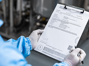
| Documentation | Material cert, inspection report, traceability needs |
| File formats | DXF for outline, STEP if 3D features, PDF with dimensions |
A typical evaluation cycle for non-standard glass orders runs 1–3 business days because suppliers may need to confirm material availability before quoting. Standard borosilicate parts can be quoted same-day.
For our internal glass cutting capability and current material range, see our glass cutting service page.
Lead Time & Logistics for Glass Parts in Singapore
Lead times for precision glass parts in Singapore vary widely by material and complexity:
| Order Type | Typical Lead Time | Driver |
|---|---|---|
| Standard borosilicate (in stock) | 3–7 working days | Cutting + inspection only |
| Quartz / fused silica | 1–2 weeks | Material may need to be ordered |
| Sapphire | 2–4 weeks | Material lead time + slower cutting |
| MCG / chemically tempered | 2–4 weeks | Specialty material procurement |
| Urgent prototype (in-stock material) | 48–72 hours | Subject to capacity |
Three logistics points that matter for glass parts that don’t matter as much for metal:
- Packaging — Anti-static foam, cleanroom packing, or ESD-safe materials may be required depending on end-use. Specify upfront.
- Handling instructions — Glass parts are far more fragile than metal in transit. Heavy parts need cushioned crates; thin parts need flat carriers.
- Documentation — Material certs, dimensional inspection reports, and cleanliness certificates are often part of the delivered package — confirm with the supplier whether these are included or extra-cost.
For our standard logistics workflow and turnaround commitments, see our logistics and lead time page.
Frequently Asked Questions
What’s the difference between glass cutting and glass dicing?
“Cutting” generally refers to separating glass into individual parts, often with curved or complex contours. “Dicing” specifically refers to separating wafer-scale substrates into many small identical dies in a regular grid, typical of semiconductor wafer processing. Dicing uses similar laser technology but is optimised for throughput and yield across hundreds or thousands of identical parts per wafer.
Can you cut chemically tempered glass without breaking it?
Yes, but only with picosecond or femtosecond lasers. The compressive surface stress that gives tempered glass its strength also makes it shatter unpredictably when cut by traditional methods. Ultrafast laser cutting uses ablation rather than thermal stress, allowing controlled separation. Cutting tempered glass on a CO₂ or even UV nanosecond laser typically results in catastrophic fracture.
What’s the minimum feature size for laser glass cutting?
For UV nanosecond lasers, minimum feature size is typically 100–200 µm. Picosecond pushes this to ~50 µm. Femtosecond can achieve sub-50 µm features for specialised applications. Holes and slots can be smaller than free-standing features because of structural support during cutting.
How is sapphire cutting different from regular glass cutting?
Sapphire is single-crystal aluminium oxide, not amorphous glass. Its extreme hardness (Mohs 9) and crystal orientation make thermal cutting methods unreliable — they tend to crack along crystal planes. Practical sapphire cutting requires ultrafast lasers (picosecond or femtosecond) that ablate material faster than heat can propagate. Cost per cut is typically 5–10× higher than borosilicate.
Do you provide ESD-safe and cleanroom-compatible packaging?
For semiconductor and medical-device parts, ESD-safe foam, anti-static bags, and cleanroom-prepared packaging are typically available on request. Specify the end-use application and required cleanliness level (e.g. ISO Class 7 / Class 10,000) when requesting a quote so the supplier can prepare appropriate packaging from the start.
Can precision glass cutting handle Class 100 / Class 1000 cleanroom-quality parts?
Yes, but the requirement needs to be specified upfront. Cleanroom-quality glass parts require not just cleanroom-compatible packaging but also controlled cutting environments, post-cut cleaning protocols (typically with deionised water and isopropanol), and certified inspection. Lead time and cost both increase compared to standard industrial-grade processing.
Get an Expert Assessment in 24 Hours
Three takeaways from this guide:
- Match material to laser technology first — sapphire and tempered glass demand ultrafast lasers; borosilicate has more options.
- Specify edge chip and tolerance explicitly — “precision glass cutting” without numbers means nothing.
- Lead times scale with material rarity — borosilicate days, sapphire weeks. Plan accordingly.