Singapore is home to one of Asia’s most sophisticated semiconductor ecosystems — from wafer fabrication to advanced packaging and equipment manufacturing. At every layer of this ecosystem, PI film serves as a critical electrical insulator, flexible substrate, and thermal barrier. Getting the cutting process right is not a quality preference — it is a production requirement.
1. Where PI Film Appears in Semiconductor Manufacturing
Polyimide film’s combination of ultra-thin form factor, thermal stability to 260°C continuous, and excellent dielectric properties makes it structurally indispensable in semiconductor production at multiple levels of the supply chain.
Wafer Chuck Insulators
PI film discs and rings serve as dielectric isolation layers in electrostatic chuck assemblies, preventing current leakage between the chuck electrode and the chamber structure. Dimensional accuracy of the insulating ring directly affects chucking uniformity and wafer edge exclusion.
Probe Card Substrates
In wafer-level test, PI film provides the flexible backing for fine-pitch probe arrays. Cutting accuracy at the probe opening determines contact registration — a few micrometres of positional error translates directly into probe yield loss at the tester.
FPC and Flex Circuit Bases
Flexible printed circuits used in semiconductor test handlers, pick-and-place machines, and bonding equipment are built on PI film substrates. The film outline cut determines board-edge clearance in tight mechanical assemblies.
EMI Shielding Films
PI-backed conductive foil assemblies protect sensitive signal traces in high-frequency semiconductor test environments. Cut-edge quality at the foil boundary determines whether electromagnetic isolation is maintained or compromised by edge fraying.
Tape Automated Bonding (TAB)
TAB carriers use PI film as the structural support for fine copper lead frames that connect bare die to substrates in high-density packages. The film sprocket holes and lead window cut accuracy drives registration through the bonding process.
Process Chamber Seals & Gaskets
In high-temperature deposition and etch equipment, PI film gaskets and insulating rings isolate chamber sections while surviving repeated thermal cycling. Dimensional consistency across a production lot ensures uniform compression and leak-tight sealing.
for probe card openings
processing on PI film
without tooling cost
2. The Precision Requirements at Each Application Layer
Not all PI film applications in semiconductor manufacturing carry the same tolerance requirement — but all of them are tighter than general industrial fabrication, and some approach the limits of UV laser capability.
| Application | Typical Tolerance | Critical Quality Factor |
|---|---|---|
| Wafer chuck insulator rings | ±0.05mm | Concentricity, edge perpendicularity |
| Probe card openings | ±0.02–0.03mm | Position accuracy of each opening |
| FPC board outline | ±0.05mm | Board-edge clearance, no delamination |
| EMI shielding film | ±0.1mm | Burr-free edge, no foil fraying |
| TAB carrier sprocket holes | ±0.02mm | Pitch consistency across full reel length |
| Chamber seals | ±0.1mm | Dimensional consistency across lot |
3. What Happens When Cutting Quality Fails
In semiconductor manufacturing, a cutting defect in a PI film component does not stay local. It propagates through the assembly and test process, multiplying in cost at every stage it goes undetected.
Dimensional non-conformance discovered at incoming inspection — the best case. The lot is rejected and returned. Lead time is lost; a replacement order is placed. Disruption is contained, but schedule impact is real.
Delamination discovered during assembly — more expensive. The PI film component has already been incorporated into a sub-assembly. Rework or discard of the partially assembled unit is required. Depending on the assembly, surrounding components may be damaged during disassembly.
Carbonized edge causing electrical leakage in service — the worst case. A PI film insulator with a carbonized cut edge passes visual inspection and may even pass initial electrical test, only to exhibit intermittent leakage at operating temperature. In a wafer processing environment, this can cause yield loss on dozens of wafers before the root cause is identified. The investigative and downtime cost far exceeds the value of the original component.
“A $15 PI film insulator cut with the wrong process can cause $50,000 in wafer yield loss before anyone finds the problem. The process selection is not a cost decision — it’s a risk decision.”Lumen Future Engineering Team · Singapore
4. How UV Cold Processing Meets Semiconductor Standards
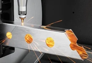
UV laser at 355nm ablates PI film through direct photon-bond breaking — the photoablation mechanism that removes material without thermal conduction into the surrounding substrate. The practical results for semiconductor applications are:
Zero adhesive reflow. Multi-layer PI film stacks — film, adhesive, and carrier — are cut without the adhesive softening beyond the cut line. Bond-line integrity is maintained, which is critical for TAB carriers and EMI film assemblies where adhesive contamination of the functional area would cause rejection.
No carbonization. The UV photoablation mechanism produces a clean, white polymer edge with no carbon residue. This is non-negotiable for dielectric applications where a conductive edge deposit would create leakage paths.
Sharp internal corners. Probe card openings and TAB windows require precise rectangular or shaped apertures with sharp corners. UV laser maintains corner sharpness to radii below 0.05mm — impossible with thermal processes that over-burn at deceleration points.
Batch consistency. UV laser cutting is CNC-programmed from your CAD file and executed identically on every part. Piece-to-piece positional variation is driven by machine repeatability — typically ±0.01–0.02mm — not by operator technique.
5. Our Workflow for Electronics Industry Clients
Semiconductor supply chains operate on tight schedules with zero tolerance for documentation gaps. Our workflow for electronics and semiconductor clients reflects this:
Engineering review before cutting. We review your PI film stack specification — film type, thickness, adhesive grade, and carrier layer if present — before confirming process parameters. Different film compositions require adjusted UV laser settings; we do not apply a one-parameter-fits-all approach.
Sample cuts with inspection report before batch confirmation. For new part numbers, we provide physical sample cuts with dimensional inspection data before the production batch is confirmed. This is standard practice — not an upgrade option.
Full documentation package. Every shipment includes material certificate for the PI film stock, dimensional inspection report, and certificate of conformance. FAI reports are available on request and included as standard for regulated applications.
MOQ of one. There is no tooling to amortise with UV laser cutting. Engineering prototyping quantities of one to ten pieces are processed on the same equipment and to the same quality standard as production volumes.
Processing PI Film for a Semiconductor Application?
Send us your film stack specification and drawing. We will confirm process suitability and provide sample cuts with inspection data within 48 hours.
Request a Sample Cut →