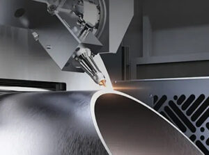
PI film (polyimide) is too thin and thermally sensitive for standard fiber or CO₂ laser cutting. Both leave a heat-affected zone (HAZ) that causes delamination, charring, and dimensional inconsistency. UV laser cold processing ablates material without heat transfer — producing burr-free, delamination-free edges that meet electronics-grade quality standards. For FPC, EMI shielding film, and flexible insulators, UV cold processing is not a premium option. It is the baseline requirement.
- What Is PI Film and Where Is It Used?
- Why PI Film Is Uniquely Difficult to Cut
- Cutting Method Comparison: Die / Fiber / CO₂ / UV
- How UV Cold Processing Works
- The 4 Defects That Ruin PI Film Parts — and How UV Prevents Them
- Key Applications in Singapore’s Electronics Supply Chain
- What to Ask Your Fabricator Before You Order
1. What Is PI Film and Where Is It Used?
Polyimide (PI) film — commonly known by the trade name Kapton® — is a high-performance engineering polymer that has become indispensable in electronics manufacturing. Its combination of thermal stability (continuous use up to 260°C), excellent dielectric properties, dimensional stability, and extreme thinness makes it irreplaceable in applications where other materials simply cannot perform.
Flexible Insulators
Dielectric layers in power modules, motor windings, and transformer coils
FPC Substrates
Base material for flexible printed circuits in smartphones, wearables, cameras
EMI Shielding Film
Electromagnetic interference barriers in PCB assemblies and RF modules
Coverlay Film
Protective overlay bonded to the copper traces of flexible circuits
Stiffeners
Localized rigidity backing in FPC connector zones to prevent fatigue failure
Heater Elements
Encapsulation for etched-foil resistance heaters in aerospace and medical devices
In Singapore’s context, PI film components appear throughout the semiconductor equipment supply chain, consumer electronics manufacturing, and precision medical device assembly — three of the island’s most strategically important industries. Getting the cutting process right is not a secondary concern. It directly determines whether your components pass incoming inspection at your customer’s facility.
commonly processed
temperature rating
UV cold processing
2. Why PI Film Is Uniquely Difficult to Cut
PI film presents a set of properties that make conventional cutting — mechanical or thermal — extremely challenging:
Extreme thinness. Most production PI film runs from 0.025mm to 0.125mm thick. At these dimensions, any mechanical contact from a blade or punch creates stress concentrations that cause tearing, dimensional shift, and delamination at the adhesive layer — particularly when cutting multi-layer film stacks.
Thermal sensitivity of the adhesive layer. PI film is almost always used with an acrylic or epoxy adhesive backing. While the PI polymer itself has excellent heat resistance, the adhesive layer begins to degrade at temperatures well below the PI’s rating. Any cutting process that transfers heat into the cut zone — even briefly — risks softening, bubbling, or reflow of the adhesive, which permanently distorts the part geometry.
Tendency to absorb and retain heat. Despite its excellent thermal properties in service, PI film absorbs laser energy efficiently. With longer-wavelength lasers (fiber or CO₂), this energy cannot be removed fast enough before it spreads laterally into the surrounding material, creating the heat-affected zone that causes downstream failures.
Tight geometric tolerances. FPC outlines, coverlay cutouts, and insulator perforations are typically specified to ±0.05mm or tighter. Achieving this consistently across a production batch — not just a prototype — requires a non-contact, thermally neutral cutting process with submicron repeatability.
3. Cutting Method Comparison
There are four methods commonly offered for PI film cutting. Here is an honest assessment of each:
| Method | Edge Quality | HAZ | Prototype Suitability | Production Suitability |
|---|---|---|---|---|
| Die Cutting / Punch | Acceptable on simple shapes | None (mechanical) | Not viable — tooling cost | High volume only; no flexibility |
| CO₂ Laser | Charred, brittle edges | Severe — wide burn zone | Not recommended | Not suitable for electronics |
| Fiber Laser | Better than CO₂, still thermal | Present — adhesive reflow risk | Possible for non-critical parts | Insufficient for electronics-grade |
| UV Laser (355nm) | Clean, burr-free, sharp corners | <5μm — negligible | Ideal — no tooling required | Production standard for FPC/PI |
| Ultrafast (ps/fs) Laser | Exceptional — near-zero HAZ | Essentially zero | Best for ultra-fine features | Higher cost; reserved for critical apps |
“Die cutting requires expensive tooling and locks you into a fixed geometry. CO₂ and fiber lasers leave thermal damage that fails electronics inspection. UV laser cold processing is where prototype flexibility meets production quality.”Lumen Future Engineering Team · Singapore
4. How UV Cold Processing Works
Understanding why UV laser processing is so different from fiber or CO₂ requires a brief look at the physics — because this is not just a marketing distinction. The mechanism of material removal is fundamentally different.
With fiber laser (1,064nm) and CO₂ laser (10,600nm), the longer wavelength means lower photon energy per quantum. The material absorbs the energy as heat, which conducts laterally before the material can be removed. This is the heat-affected zone — and on PI film, it is not a cosmetic issue. It is a structural failure.
UV laser at 355nm carries roughly three times the photon energy of a fiber laser. This is sufficient to directly break the polymer backbone bonds of polyimide through a process called photoablation — the material is removed molecule by molecule, not melted away. The thermal load on surrounding material is measured in micrometres, not millimetres.
This is what enables UV cold processing to achieve the clean, sharp-cornered outlines that electronics manufacturing demands — including internal cutouts, complex perforations, and fine slot geometries — with ±0.05mm positional accuracy across a full production batch.
5. The 4 Defects That Ruin PI Film Parts — and How UV Prevents Them
Defect 1: Adhesive Reflow
When heat from a fiber or CO₂ laser reaches the adhesive layer, the acrylic or epoxy binder softens and flows laterally beyond the cut edge. The result is an uneven adhesive bead, contamination of the cut perimeter, and compromised bonding when the part is laminated into the assembly. UV cold processing keeps the cut zone below the adhesive’s glass transition temperature, so the bond line remains crisp and dimensionally accurate.
Defect 2: Edge Delamination
Multi-layer PI film stacks — for example, PI film + adhesive + copper foil — are particularly vulnerable to thermal delamination. Heat causes differential expansion between layers, and the interfacial adhesive fails. Parts may appear intact until they are subjected to the thermal cycling of reflow soldering or in-service operation, where the delaminated zone propagates catastrophically. UV processing removes each layer without heating the interface.
Defect 3: Carbonization (Charring)
CO₂ laser cutting of PI film consistently produces a dark, carbon-rich residue along the cut edge. This carbonized layer is electrically conductive — a serious problem in applications where the PI film is serving as a dielectric insulator. Even partial carbonization can create leakage paths that cause intermittent electrical failures in service. UV cold processing leaves a clean, white polymer edge with no carbon residue.
Defect 4: Dimensional Drift at Corners
Sharp internal corners are among the most demanding features in PI film cutting. Thermal lasers tend to over-burn at corners where the beam decelerates — a phenomenon called “corner rounding” — which causes the internal geometry to deviate from the design intent. UV laser systems, with their cold ablation mechanism and high beam quality, maintain corner sharpness down to radius dimensions below 0.1mm.
6. Key Applications in Singapore’s Electronics Supply Chain
Singapore’s electronics and semiconductor manufacturing ecosystem is one of the most advanced in the world — and it places exacting demands on component suppliers at every tier.
Semiconductor equipment components. Wafer handling systems, probe card assemblies, and test socket insulators frequently use PI film as a dielectric spacer or insulating layer. Dimensional tolerance and electrical integrity requirements at this level make UV cold processing non-negotiable. A carbonized edge or delaminated layer discovered during incoming inspection means rejection, re-order delays, and schedule disruption on a production line that operates 24/7.
Consumer electronics and wearables. Smartphones, earbuds, smartwatches, and cameras contain multiple FPC assemblies with PI film substrates, coverlays, and stiffeners. As device geometries continue to shrink, the feature sizes required in PI film cutting have moved from millimetre-scale to sub-millimetre — a territory only reachable with UV laser precision.
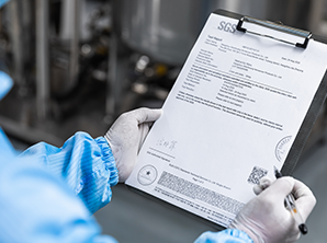
Medical devices. Implantable and wearable medical electronics rely on PI film for its biocompatibility, flexibility, and thermal stability. Regulatory requirements in this sector additionally demand full traceability documentation — material certificates, dimensional inspection reports, and process records — for every production lot.
EMI shielding solutions. EMI shielding film stacks — typically PI film bonded to metallic foil — must be cut to board outline with tight registration to mounting features. Any burr or delamination along the cut edge compromises shielding effectiveness and can interfere with the assembly process.
7. What to Ask Your Fabricator Before You Order
Not every vendor who claims to cut PI film is using a UV cold process. Some use standard fiber lasers with adjusted parameters and describe the result as “laser cutting” — which is technically accurate but omits the critical detail of thermal damage. Here is how to qualify your fabricator before committing production volume:
-
Ask: “What laser wavelength do you use for PI film?” — The answer should be 355nm (UV) or ultrafast (picosecond/femtosecond). If the answer is 1,064nm (fiber) or 10,600nm (CO₂), ask specifically how they manage the HAZ.
-
Request a cut sample on your specific film stack. Prototype cut samples on your exact material combination — PI thickness, adhesive type, and any carrier layer — are the only meaningful proof of capability. Generic samples on different materials do not transfer.
-
Ask for a cross-section image of the cut edge. A properly UV-processed PI film edge should show a clean, perpendicular cut with no visible HAZ under 10× magnification. Charring or adhesive reflow will be visible at 5×.
-
Confirm dimensional capability with data. Ask for a dimensional report from a recent PI film job showing measured edge-to-feature positional accuracy. Look for ±0.05mm or better across the batch, not just on a single piece.
-
Verify documentation availability. For regulated applications (medical, aerospace, semiconductor), confirm that material certificates, FAI reports, and lot traceability records will accompany the shipment.
-
Ask about minimum order quantity. UV laser cutting requires no tooling — a competent fabricator should be able to process from 1 piece for prototyping without a setup surcharge that makes sampling uneconomical.
Processing PI Film, FPC, or Specialty Films?
Our UV cold processing line is dedicated to electronics-grade film cutting. Submit your film stack specifications and we will provide a sample cut and dimensional report within 48 hours.
Request a Sample Cut →