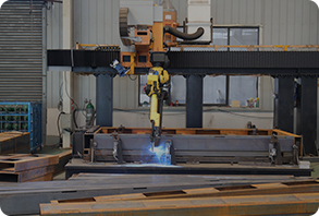
PI film (polyimide, often called Kapton) is laser cut using UV lasers — and increasingly UV picosecond lasers — because they deliver micron-level precision, clean edges with no burrs, no mechanical stress, and minimal carbonization (the black charred residue that ruins electrical insulation). Laser cutting suits FPC outlines, depaneling, coverlay openings, and stiffeners. Unlike die cutting, it needs no tooling, making it faster and cheaper for prototypes and small-to-medium batches. For FPC engineers in Singapore, local laser cutting can replace the 2–3 week round trip of sending parts overseas.
If you design flexible circuits or work in electronics manufacturing in Singapore, you’ve probably hit this wall: you need PI film or FPC parts cut to a precise shape for a prototype, and your options are to send the job overseas (and wait 2–3 weeks) or find one of the very few local suppliers who actually understand polyimide cutting.
This guide is for FPC engineers, semiconductor packaging engineers, and electronics procurement teams who need to understand how PI film laser cutting actually works — what materials can be cut, how to avoid the carbonization that ruins parts, when laser beats die cutting, and what precision is realistic. We’ve kept the engineering depth but explained each term as it comes up, so procurement readers can follow along too.

If you’re new to laser fabrication generally, our complete laser cutting buyer’s guide is a good primer. And if you also work with brittle materials, our companion precision glass cutting guide covers the other half of the electronics materials world.
What Is PI Film, and Why Laser Cut It?
PI film — polyimide film, most commonly known by DuPont’s brand name Kapton — is a thin, flexible, amber-coloured plastic film that’s exceptionally good at two things: surviving heat and insulating electricity. It stays stable from cryogenic temperatures all the way up to around 400°C, resists most chemicals, and bends without breaking. That combination makes it the backbone of flexible printed circuits (FPCs), insulation layers, and a wide range of electronics components.

So why cut it with a laser instead of a blade or a die (a metal stamping tool)? Four reasons matter to engineers:
- No mechanical stress — A laser is a beam of light, not a physical tool. It doesn’t push, tear, or deform the thin film the way a blade or punch can.
- No burrs, clean edges — Mechanical cutting leaves rough edges; laser cutting leaves smooth ones, which matters for reliability in tight assemblies.
- No tooling required — Die cutting needs a custom-made die that costs hundreds to thousands of dollars and takes days to make. A laser just needs your design file, so prototypes happen same-week.
- Micron-level precision and complex shapes — Lasers cut intricate geometries, tiny holes, and fine features that physical tools can’t match.
The catch — and the rest of this guide deals with it — is that cutting PI film badly produces carbonization, the black charred residue that compromises both appearance and electrical performance. Getting clean cuts is about choosing the right laser and the right parameters.
The Materials You Can Laser Cut in the FPC Stack
A flexible circuit isn’t just one material — it’s a “stack” of several layers, and laser cutting touches most of them. Here’s what each layer is and what to watch for when cutting it:
| Material | What It Does | Typical Thickness | Cutting Consideration |
|---|---|---|---|
| PI / Kapton film | Base substrate and insulation layer | 12.5–125 µm | Avoid carbonization with UV laser |
| FCCL (flexible copper-clad laminate) | PI film bonded with copper foil — the circuit base | Varies (includes copper) | Requires depth control to avoid cutting copper |
| Coverlay | Protective film laminated over the circuit | 12.5–50 µm | Precise window openings over pads |
| PI Stiffener | Rigid backing for component mounting areas | 100–300 µm | Must cut cleanly through thicker material |
| EMI shielding film | Blocks electromagnetic interference | Thin, multi-layer | Cut without damaging layers beneath |
| PSA (pressure-sensitive adhesive) | Bonding/mounting layer | Thin | Avoid melt residue and gumming |
| PET film | Lower-cost substrate alternative | Thin | Lower melting point — gentler process needed |
The takeaway: “PI film cutting” in practice often means cutting a multi-layer assembly where different layers respond differently to the laser. A supplier who only knows how to cut bare PI film may struggle with a real FPC stack. See our full materials reference for the wider list.
The Carbonization Problem (And How Lasers Solve It)
This is the single most important quality issue in PI film cutting, so it’s worth understanding clearly.
Why does this matter so much? Because that carbon residue is electrically conductive — the exact opposite of what you want from an insulating film. Carbonization along a cut edge can cause leakage currents, reduce insulation resistance, and create long-term reliability failures in the field. It also looks bad, which matters for quality acceptance.
The amount of carbonization depends almost entirely on how much heat the cutting process dumps into the material:
UV / Picosecond Laser
Short-wavelength, short-pulse lasers remove material faster than heat can spread. The edge stays clean, amber-coloured, and electrically sound. This is what high-reliability FPC work requires.
Wrong Process / Too Much Heat
A high-power CO₂ laser or wrong settings dumps heat into the film, leaving a black charred edge with conductive residue — a reliability risk and a cosmetic reject.
The practical rule: for any FPC or insulation application where electrical performance matters, the cutting process should be chosen specifically to minimize the heat-affected zone (HAZ) — the region around the cut where the material’s properties have been changed by heat. The next section explains which lasers do this best.
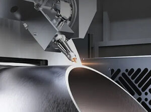
Laser Technologies for PI Film: CO₂ vs UV vs Picosecond
Three laser types are used on PI film, with very different results. Here’s how they compare:
CO₂ Laser (10.6 µm wavelength)
The most common and cheapest industrial laser. It cuts PI film by melting and burning, which means more heat — and therefore more carbonization and a larger heat-affected zone. Acceptable for thick PI parts or rough cuts where electrical performance isn’t critical, but generally not the right choice for precision FPC work.
- Best for: Thick PI sheets, rough cutting, non-critical insulation parts
- Weakness: Higher carbonization, larger HAZ
UV Nanosecond Laser (355 nm wavelength)
Short ultraviolet wavelength breaks molecular bonds more directly with less heat — often called “cold cutting” even though it isn’t truly heat-free. This is the workhorse for most FPC and PI film cutting, balancing quality, speed, and cost.
- Best for: FPC outlines, coverlay openings, most PI film parts
- Weakness: Some HAZ on very heat-sensitive or ultra-thin parts
UV Picosecond Laser (extremely short pulses)
The premium option. Pulses so short (trillionths of a second) that material is removed before heat has time to spread into the surrounding film. Produces near-zero carbonization and the cleanest possible edges. Used for the most demanding applications — fine micro-holes, ultra-thin films, high-reliability electronics.
- Best for: Precision micro-features, ultra-thin film, high-reliability and medical electronics
- Weakness: Slower and higher cost per part than UV nanosecond
Matching PI film application to laser technology
Laser Depth Control: Cutting Coverlay Without Damaging Copper
This is one of the most useful — and technically demanding — capabilities in FPC laser cutting, and it’s worth explaining in plain terms.
How is this possible? It relies on the fact that PI film and copper respond differently to certain laser wavelengths, combined with precisely controlled pulse energy. The laser is tuned to remove the polymer layer efficiently while leaving the reflective copper beneath essentially untouched. Some processes also use real-time monitoring to detect when the copper layer is reached.
Why FPC engineers care about this:
- Pad exposure — Opening windows in the coverlay to expose contact pads for soldering or bonding
- Dual-access flex circuits — Accessing copper from both sides of the circuit
- Selective layer removal — Removing specific layers in a multi-layer stack without affecting others
This kind of selective, depth-controlled processing is extremely difficult with mechanical methods, which is a major reason laser cutting has become standard for advanced flexible circuits.
Laser Cutting vs Die Cutting: When to Use Each
For procurement and engineering decisions, this is the key comparison. Die cutting (using a custom metal stamping tool) and laser cutting each have a clear sweet spot:
| Factor | Laser Cutting | Die Cutting |
|---|---|---|
| Tooling cost | None | High (custom die, hundreds to thousands of $) |
| Prototype speed | Fast — design file only | Slow — wait for die fabrication |
| Per-piece cost (high volume) | Higher | Lower |
| Precision | Micron-level | Moderate |
| Minimum feature size | <50 µm (picosecond) | Limited by tool geometry |
| Design changes | Instant (edit the file) | New die required |
| Best batch size | Prototype, small-to-medium batch | Large-volume production |
The decision rule is simple: Use laser cutting for prototypes, design iterations, small-to-medium batches, and anything with fine features or frequent design changes. Switch to die cutting once you’re in stable, high-volume production where the per-piece savings outweigh the upfront tooling cost. Many products move from laser (prototype phase) to die (mass production) over their lifecycle — and laser cutting is what gets you to market fast.
Achievable Precision & Quality Standards
Industry-typical performance for PI film laser cutting by technology. Use these as reference benchmarks when specifying a project — actual results depend on material, thickness, and the specific equipment:
| Laser Technology | Kerf Width (cut width) | Position Accuracy | Min. Hole Diameter | Heat-Affected Zone |
|---|---|---|---|---|
| CO₂ Laser | ~100 µm | ±50 µm | ~200 µm | Large |
| UV Nanosecond | ~30 µm | ±20 µm | ~50 µm | Small |
| UV Picosecond | ~15 µm | ±10 µm | <10 µm | Minimal |
For reference, a human hair is roughly 70 µm wide — so a picosecond laser can drill holes smaller than the width of a hair. Quality acceptance for PI film parts typically checks four things:
- Dimensional accuracy — Do the cut dimensions match the drawing within tolerance?
- Edge quality / carbonization — Is the edge clean and free of black charring? (Often checked under microscope)
- No delamination — Have the laminated layers stayed bonded at the cut edge?
- Electrical integrity — For functional circuits, does insulation resistance meet spec?
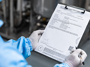
See our quality assurance process for how inspection is handled on precision parts.
Singapore FPC & Electronics Applications
PI film laser cutting supports several of Singapore’s strongest electronics and semiconductor segments:
Semiconductor Packaging
Singapore’s large semiconductor base uses PI film for insulation layers, die-attach films, and process components. Precision PI parts are needed for advanced packaging where dimensional accuracy and cleanliness are critical.
FPC / Flexible Circuit Manufacturing
The core application: cutting FPC outlines (profiling), separating individual circuits from a production panel (depaneling), opening coverlay windows, and shaping PI stiffeners. Local cutting is especially valuable during the prototype and pilot-production phases.
Consumer Electronics
Camera modules, fingerprint sensors, wearables, and foldable devices all rely on precisely cut flexible circuits and PI components. These often demand the fine features that only UV or picosecond lasers can deliver.
Automotive & Industrial Electronics
Automotive FPCs (sensors, displays, control modules) and industrial electronics need PI parts that survive heat and vibration. Reliability requirements make clean, carbonization-free edges essential.
Medical Electronics
Medical wearables, diagnostic devices, and miniaturized sensors use flexible circuits where both precision and biocompatibility matter. Documentation and traceability are usually part of the requirement.
From Design File to Cut Parts: The Prototyping Workflow
Here’s how a typical PI film cutting project flows — and why doing it locally in Singapore saves significant time:
- File preparation — Send a DXF or Gerber file with the cut outline, plus material specification (type, thickness) and quantity. For coverlay openings or depth control, mark which layers to cut.
- Process assessment — The supplier reviews material, thickness, and precision requirements to select the right laser (CO₂, UV nanosecond, or picosecond).
- Prototyping — Because no tooling is needed, prototypes can be cut quickly — often within 48–72 hours when material is in stock.
- Inspection — Dimensional check, edge quality / carbonization inspection, and electrical verification if required.
- Small batch to production — Once the prototype is approved, scale to small or medium batches with the same process — no tooling delay.
The time saving is the real story here. Sending PI film cutting overseas typically means a 2–3 week round trip including shipping and customs. Local cutting in Singapore compresses that to days — a major advantage when you’re iterating on a design or racing a product deadline. For current turnaround commitments, see our logistics and lead time page, or go straight to our PI film cutting service page.
Frequently Asked Questions
Can laser cutting damage the copper layer in an FPC?
It doesn’t have to. With laser depth control, the laser is tuned to remove only the PI/coverlay dielectric layer and stop at the copper beneath, leaving it undamaged. This is a deliberate, controlled process used for exposing pads and creating dual-access circuits. Without depth control, a full cut goes through all layers — which is what you want for outline cutting and depaneling.
How thin a PI film can be laser cut?
PI films as thin as 12.5 µm (and even thinner in some cases) can be laser cut. Very thin films are best handled with UV nanosecond or picosecond lasers, which minimize heat and avoid distorting or carbonizing the delicate material. Thicker PI stiffeners up to 300 µm are also routinely cut.
Does laser cutting PI film cause carbonization?
It can if the wrong process is used. High-heat methods like CO₂ lasers tend to leave a black carbonized edge, which is electrically conductive and undesirable for insulation. UV and especially UV picosecond lasers minimize heat input and produce clean, carbonization-free edges suitable for high-reliability electronics.
What file format do I need for PI film laser cutting?
A DXF file is standard for cut outlines. Gerber files work well for FPC-related geometry. A STEP file helps if there are 3D features. Always include material type, thickness, quantity, and — for multi-layer parts — which layers should be cut versus left intact.
Is laser cutting or die cutting better for FPC prototypes?
For prototypes, laser cutting is almost always better. It needs no custom tooling, so you avoid the cost and the days-long wait for a die to be made. You can also revise the design instantly by editing the file. Die cutting becomes more economical only at high production volumes, where the per-piece cost savings outweigh the upfront tooling investment.
Can you cut rigid-flex PCBs?
Rigid-flex PCBs (which combine rigid and flexible sections) can be laser cut, though they’re more complex than pure flexible circuits because the laser must handle different material types in one part. The flexible PI sections cut well with UV lasers; the rigid sections may need different parameters. Discuss the specific stack-up with your supplier when requesting a quote.
Get a Local PI Film Prototype in 48–72 Hours
Three takeaways from this guide:
- Carbonization is the enemy — choose a UV-based process for any part where electrical performance matters.
- Laser beats die cutting for prototypes and small batches — no tooling, no waiting, instant design changes.
- Cutting locally in Singapore saves 2–3 weeks versus sending parts overseas.